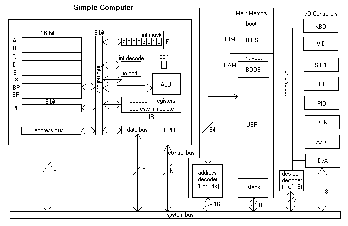
The CPU is comprised of 8, 16-bit programmer-visible registers, a 16-bit program counter (PC), a flag register, an I/O port register (4 bits), an interrupt decode register (4 bits), an acknowledge bit, a 32-bit instruction register and an arithmetic/logic unit (ALU). Additionally there is an internal 8-bit bus for all signals (address, data and control). Details of control have been suppressed to emphasize the essential features pertinent to systems programming. The memory is a 64k space of byte organized cells. The figure shows a layout for memory composed of a 2k ROM (read only memory) and 62k of RAM (volitile random access memory). Shown is a map of regions used for various system purposes. The boot and BIOS (basic input/output system) occupy ROM. from location 0 to 2048d. The next 32 bytes are dedicated to an interrupt vector table. Next an approximate area dedicated to the BDOS (basic disk operating system). The reason this area is approximate is that different versions of the OS occupy different amounts of space. The largest area is devoted to user programs (USR). This area is also approximate since it is sandwiched between the BDOS and the system stack area. Extra care is needed in establishing the boundries of these areas and making sure the user program does not extend into either of the other two areas.
The first five registers, A, B, C, D, E are general purpose, except that A is used as the accumulator. All arithmetic/logic operations results are sent to the A register. The rest of the registers are special purpose (e.g. IX for indexed addressing, BP for base addressing, and SP for stack pointer) The E register is an extra 16-bit register which is used as an adjunct to the accumulator (A) for multiplication and division arithmetic operations for double precision results.
Instruction formats
| Format 0 | 00 |
| Format 1 | 01 | dest, r1 | src, r2 |
| Format 2 | 01 | immediate |
| Format 3 | 10 | immediate high | immediate low |
| Format 4 | 11 | r1 | src, r2 | immed/addr high | immed/addr low |
Opcode decoding
Bit 7: 0 for all instructions except load/store, 1 for load/store/move
Bit 2: if bit 7 == 1: 0 = byte mode, 1 = word mode
Bits 0,1: as above, determines the number of bytes needed in the instruction
Conventions
r = A, B, C, D, E, IX, BP, SP
r' = r; F (flags, Int and I/O word)
rH = the high order 8 bits of
register r, rL is the low order 8 bits of register r. These designations
are required to designate the destination or source for 8-bit data.
addr stands for a memory address
immed stands for an immediate value
M stands for main memory.
The [] brackets indicate contents of an address in memory or contents of a register in certain cases.
neg = negative flag
carry = carry flag
ovfl = overflow flag
zero = zero flag
-1 = true
0 = false
push(r) is an internal call that accomplishes the PUSH operation on register r.
pop() is an internal call that accomplishes the POP operation into the desiganted register
| Instruction | Semantics | Example | Bytes | Hex |
| Load and Store | ||||
| LDB r, addr | rL <- M[addr] | LDB C, COUNTER | 4 | 83 |
| LD r, addr | rL <- M[addr]; rH <- M[addr+1] | LD C, COUNTER | 4 | 87 |
| LDB r, #immed | rL <- immed | LDB D, #ONE_HUNDRED | 3 | 8A |
| LD r, #immed | rL <- immed; rH <- immed+1 | LD D, #ONE_HUNDRED | 4 | 8F |
| LDB r, !addr | rL <- M[IX] ; indexed | LDB D, !INDEX | 2 | 81 |
| LD r, !addr | rL <- M[IX++]; rH <- M[IX++] | LD D, !INDEX | 2 | 85 |
| LDB r, +offset | rL <- M[BP+offset] ; base+offset | LDB D, +START_LINE | 4 | 8B |
| LD r, +offset | rL <- M[BP+offset]; rH <- M[BP+offset+1] | LD D, +START_LINE | 4 | 97 |
| LDB r, +[r'] | rL <- M[BP+[r']] ; base+reg | LDB D, +C | 2 | 89 |
| LD r, +[r'] | rL <- M[BP+[r']]; rH <- M[BP+[r']+1] | LD D, +C | 2 | 95 |
| LDB r, @addr | rL <- M[M[addr]] ; indirect | LDB D, @POINTER | 4 | 9B |
| LD r, @addr | rL <- M[M[addr]]; rH <- M[M[addr+1]] | LD D, @POINTER | 4 | 9F |
| LDB r, @r' | rL <- M[M[[r']]] ; register indirect | LDB D, @E | 2 | 99 |
| LD r, @r' | rL <- M[M[[r']]]; rH <- M[M[[r]]+1] | LD D, @E | 2 | 9D |
| MOV r, r' | r1 <- [r'] | MOV D, A | 2 | B5 |
| STB addr, r | M[addr] <- rL ; memory destination direct | STB RESULT, A | 4 | 93 |
| ST addr, r | M[addr] <- rL; M[addr+1] <- rH | ST RESULT, A | 4 | B7 |
| STB !, r | M[IX++] <- rL ; indexed (no dest operand) | STB !, A | 2 | B1 |
| ST !, r | M[IX++] <- rL; M[IX++] <- rH | ST !, A | 2 | BD |
| STB +offset, r | M[BP+offset] <- rL ; base reg + immed offset | STB +OFFSET, A | 4 | C3 |
| ST +offset, r | M[BP+offset] <- rL; M[BP+offset+1] <- rH | ST +OFFSET, A | 4 | C7 |
| STB +r', r | M[BP+[r']] <- rL ; base reg + reg | STB +C, A | 2 | C1 |
| ST +r', r | M[BP+[r']] <- rL; M[BP+[r']+1] <- rH | ST +C, A | 2 | C5 |
| STB @addr, r | M[M[addr]] <- rL ; indirect | STB @POINTER, A | 4 | CB |
| ST @addr, r | M[M[addr]] <- rL; M[M[addr]+1] <- rH | ST @POINTER, A | 4 | CF |
| STB @r', r | M[M[[r']]] <- rL ; register indirect | STB @C, A | 2 | D1 |
| ST @r', r | M[M[[r']]] <- rL; M[M[[r']]+1] <- rH | ST @POINTER, A | 2 | D5 |
| Arithmetic Logic | ||||
| COMP r2 | A <- ~r2; 2s complement neg <- A[7]; carry <- 0; ovfl <- 0; zero <- 1 if A == 0 |
COMP D | 2 | 39 |
| ADD r1, r2 | A <- r1 + r2; neg <- A[7]; carry <- 1 if r1[7] + r2[7] > 1; ovfl <- 1 if r1[7]==r2[7] AND A[7] != r1[7]; zero <- 1 if A == 0 |
ADD A, D | 2 | 01 |
| ADDC r1, r2 | A <- r1 + r2 + carry neg <- A[7]; carry <- 1 if r1[7] + r2[7] > 1; ovfl <- 1 if r1[7]==r2[7] AND A[7] != r1[7]; zero <- 1 if A == 0 |
ADDC A, C | 2 | 05 |
| SUB r1, r2 | A <- ~r2; A <- ADD r1, r2; flags set by ADD op |
SUB B, C | 2 | 09 |
| AND r1, r2 | A <- r1 & r2 ; bitwise AND neg <- A[7]; zero <- 1 if A == 0 |
AND B, D | 2 | 11 |
| OR r1, r2 | A <- r1 | r2 ; bitwise OR neg <- A[7]; zero <- 1 if A == 0 |
OR B, D | 2 | 15 |
| XOR r1, r2 | A <- r1 ^ r2 ; bitwise XOR neg <- A[7]; zero <- 1 if A == 0 |
XOR B, D | 2 | 19 |
| NOT r1 | A <- ~r1 ; bitwise NOT neg <- A[7]; zero <- 1 if A == 0 |
NOT A | 2 | 1D |
| LAND r1, r2 | A <- -1 if (r1 && r2) else 0 ; logical AND neg <- A[7]; zero <- 1 if A == 0 |
LAND B, D | 2 | |
| LOR r1, r2 | A <- -1 if (r1 || r2) else 0 ; logical OR neg <- A[7]; zero <- 1 if A == 0 |
LOR B, D | 2 | |
| LNOT r1 | A <- -1 if (!r1) else 0 ; logical NOT neg <- A[7]; zero <- 1 if A == 0 |
LNOT C | 2 | |
| Data Manipulation | ||||
| SHL r | A <- r * 2; neg <- A[7]; carry <- r[7] before shift; zero <- 1 if A == 0 |
SHL D | 2 | 21 |
| SHR r | A <- r / 2; neg <- 0; carry <- r[0] before shift; zero <- 1 if A == 0 |
SHR D | 2 | 25 |
| ROTL r1 | A <- r * 2; r[0] <- carry neg <- A[7]; carry <- r[7] before rotate; zero <- 1 if A == 0 |
ROTL D | 2 | 29 |
| ROTR r1 | A <- r / 2; r[7] <- carry neg <- A[7]; carry <- r[0] before rotate; zero <- 1 if A == 0 |
ROTR D | 2 | 2D |
| Flow Control | ||||
| JMP r | PC <- [r] | JMP D | 2 | 41 |
| JMP immed | PCL <- immed; PCH <- immed+1 | JMP LOOP1 | 3 | 42 |
| JMPx r [x=N,C,O,Z] | PC <- [r] | JMPZ D | 2 |
N 4D C 49 O 46 Z 45 |
| JMPx immed | PCL <- immed; PCH <- immed+1 | JMPZ LOOP1 | 3 |
N 56 C 52 O 5A Z 4E |
| CALL r | push(PC); PC <- [r] | CALL D | 2 | 51 |
| CALL immed | push(PC); PCL <- immed; PCH <- immed+1 | CALL CHECK_RESULT | 3 | 5E |
| RET | PC <- pop(SP) | RET | 1 | 50 |
| RETI | flags <- pop(SP); PC <- pop(SP) | RETI | 1 | 54 |
| PUSH r | M[SP]<- rH; SP <- SP-1; M[SP]<- rL; SP <- SP-1 | PUSH A | 2 | 55 |
| POP r | SP <- SP+1; rL <-M[SP]; SP <- SP+1; rH <-M[SP] | POP A | 2 | 5D |
| PUSHB r | M[SP]<- rL; SP <- SP-1 | PUSH A | 2 | 55 |
| POPB r | SP <- SP+1; rL <- M[SP]; | POP A | 2 | 5D |
| I/O | ||||
| IN r | rL <- Port[F[3..0]] | IN B | 2 | 69 |
| OUT r | Port[F[3..0]] <- rL | OUT B | 2 | 6D |
| SETP immed | F[3..0] <- immed | SETP 3 | 2 | 71 |
| Miscellaneous | ||||
| NOP | no operation | NOP | 1 | 00 |
| HALT | stops the computer (run bit <- 0) | HALT | 1 | 04 |
| ESC | indicates next instruction is FPU instruction if FPU present | ESC | 1 | 08 |
| SIM immed | F[11..8] <- immed[3..0]; set interrupt mask | SIM 0x03 | 2 | 31 |
| EI | inables interrupts | EI | 1 | 30 |
| DI | disables interrupts | DI | 1 | 34 |
| EOI | end of interrupt processing | EOI | 1 | 38 |
| TRAP immed | generates software interrupt at vector offset, immed | TRAP #13 ; call trap routine at offset 13 decimal | 2 | |